Marktech Optoelectronics
3 Northway Lane North
Latham, NY 12110
Fax: +1-785-4725
Email: in**@ma**********.com
The broadest line of both silicon and InGaAs detectors commercially available.
Indium Gallium Arsenide (InGaAs) PIN photodiodes are made using InGaAs/InP technology.
Cutting-edge silicon photodetectors that excel in precise detection of light ranging in wavelength from 250nm to 1100nm
Monolithic “quads” or quadrant photodiodes (QPDs) are 2 X 2 photodiode arrays with four planar diffused photodiode elements or segments.
Marktech offers a broad line of silicon photo Transistors in a variety of package types ranging from miniature metal can to ceramic packages.
Our High-Reliability Photoreflectors are sensors that contain both the LED emitter and photodetector functions within a single package.
Marktech Si APD’s offer low-level light and short pulse detections of wavelengths between 400 nm and 1100 nm.
UV detectors are offered in a variety of TO metal-can type packages from TO-18 to TO-39 with special UV glass lens to insure optimum lifetime and the least amount of material degradation
With the ability to detect light in the UV, visible, and infrared spectrums, photo detectors, photo transistors, and photodiodes are being used in increasingly more applications.
Marktech offers the broadest range of emitters commercially available ranging from 235nm to 4300nm across the UV, visible, NIR, SWIR, and MWIR spectral ranges.
Marktech offers the broadest range of UV LEDs commercially available ranging from 235nm to 400nm including UVA, UVB, UVC, and deep UVC LEDs.
Our advanced line of visible LED products is engineered to deliver high-quality, energy-efficient lighting solutions across various applications from 400nm to 700nm..
Our NIR LED wavelength range is typically from 700nm to 1000nm, extending into wavelengths invisible to the human eye but crucial for numerous technological and scientific applications.
Our standard product offering includes wavelengths from 1020nm to 3000nm and operating currents ranging from 20mA to 350mA for high-power applications.
Our Point Source LEDs are specifically engineered for optical encoders, edge sensors, and other critical applications that demand highly focused light with minimal dispersion.
Multi-LED chips in a single package, our multiple wavelength LEDs are engineered to address a myriad of applications across the UV, visible, NIR, SWIR, and MWIR spectral ranges
Designed to produce a highly defined red dot or reticle, facilitating accurate aiming without revealing the location to the target.
Ideally suited for applications including edge sensing, line sensing, coin bill validation, and bar code reading
Our panels are crafted to deliver uniform, vibrant illumination across a wide range of applications, from consumer electronics to industrial displays.
Crafted with the latest LED technology, these rings provide adjustable illumination to meet specific needs, ensuring optimal visibility and enhancing the quality of your projects.
As a proud CREE LED Solution Provider for over a decade, Marktech offers comprehensive engineering support, including design, binning, and material selection, alongside custom packaging options for specialized applications.
CREE LED through-hole emitters, designed for high-temperature and moisture environments with UV-resistant optical-grade epoxy, offer a range of colors for versatile applications in signage and lighting.
CREE High Brightness (HB) SMD LEDs are the brightest, most reliable architectural, video, signage, scoreboard, roadway, and specialty LEDs available today.
CREE LED’s P4 series represents a leap in LED design, combining efficiency with aesthetic versatility to meet the demands of modern lighting applications.
Marktech’s CREE LED XLamp® offerings on aluminum core starboards simplify LED integration for designers, providing a range of colors and angles on compact boards for easy testing and implementation in varied lighting applications.
Marktech Optoelectronics introduces its new product line of CREE LED die, including the EZ1350 Series Die, packaged in TO-cans (TO-18 and TO-39 outlines) designed for precision and reliability in demanding applications with protection against environmental factors like moisture and dust.
Marktech Optoelectronics combines over 40 years of expertise in optoelectronics with a focus on customized engineering solutions, addressing specific customer needs and applications.
Custom photodiode detectors are designed to meet unique customer requirements, offering specialized performance features and cost savings through optimizations such as integrated filters, photodiode arrays, and hybridization.
Through our vertically integrated manufacturing facilities in California and Japan, we offer custom LED solutions, including packaging and optoelectrical categorization, enhancing product design and market readiness.
Multiple LED dies combined in a single package are engineered to address various applications across the UV, visible, NIR, SWIR, and MWIR spectral ranges.
To succeed, you need the exact optoelectronic package custom-designed and manufactured for your application, including hermetic metal SMD, TO-can, plastic SMD, and molded through-hole packaging.
Made-to-order semiconductor chips (die) and wafers are designed and fabricated to fit your needs. Standard dies are available in specific wavelengths for high-volume production applications.
Bare and encapsulated LEDs, photodiodes, and other components are assembled on FR4, metal-cored, and flexible circuit boards, ready for production.
Learn about the latest trends, devices, and potential applications.
The latest news and announcements from Marktech Optoelectronics.
Detailed information about common uses for Marktech Optoelectronics devices.
In depth discussions on LEDs, Detectors and the science behind them.
Become familiar with common terminology and concepts for LED Devices.
List of common concepts and definitions for Photodiodes.
In addition, Marktech’s packages include Star Boards, linear boards, Multi-Chip metal cans that hold up to 7 chips, Light Rings, and many more.
Combined with our broad range of emitter and detector chip selections, we can offer more options than practically anyone.
Marktech can also tailor an LED emitter’s viewing angle or photodiode detectors’ angular sensitivity by selecting standard or custom lens types. Optical filters or filtering lenses can also be utilized to fine-tune characteristics for spectroscopy applications.
When designing your custom emitter or detector component, choose from the following optoelectronic package options.

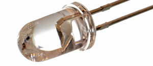
Molded through-hole packaging involves encasing optoelectronic components in a plastic body with leads that extend through the circuit board for soldering. This type of packaging is designed for applications where components need to be mounted through holes drilled into PCBs (Printed Circuit Boards). It’s durable and offers reasonable protection against environmental factors, making it suitable for applications in a dry and gas-free environment and many disposable or single-use applications. Marktech offers three and 5-mm plastic through-hole packaged LEDs and detectors.

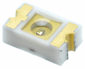
SMD packaging allows components to be mounted directly onto the surface of PCBs without the need for through holes. This packaging is characterized by its small size and low profile, which enables high-density mounting and makes it ideal for compact electronic devices. SMD packaging improves manufacturing efficiency and is widely used in modern electronic manufacturing for various optoelectronic components. Plastic-leaded SMD packaging is better than through-hole packaging for high-volume assembly processes. Like through-hole packaging, plastic SMD packaging is not airtight, so the LED or photodiode semiconductor components inside the package may degrade in applications with high moisture, volatile compounds, or industrial gases.
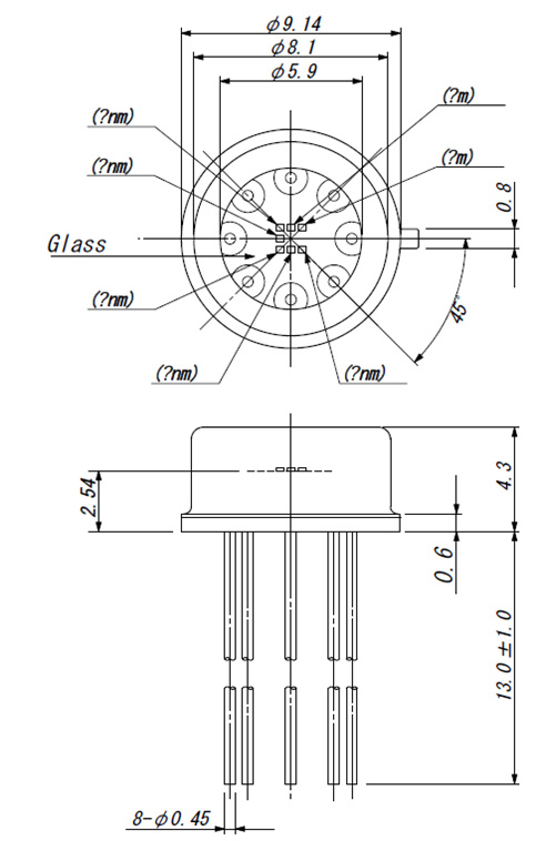
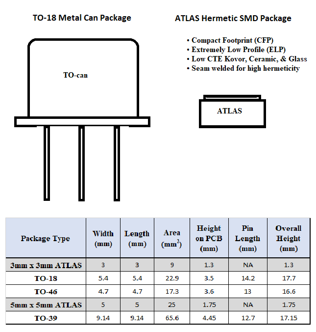
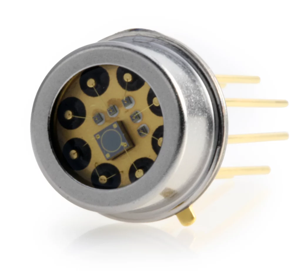
Hermetic TO-can packaging is designed to provide high protection against moisture and other environmental conditions. “TO” stands for “Transistor Outline” and refers to a sealed metal can package to ensure no gas or moisture can enter. This type of packaging is often used for sensitive optoelectronic devices, such as lasers and photodiodes, where maintaining the integrity of the internal atmosphere is critical. TO-5, T0-18, TO-39, and TO-46 cans are standard sizes we routinely work with.
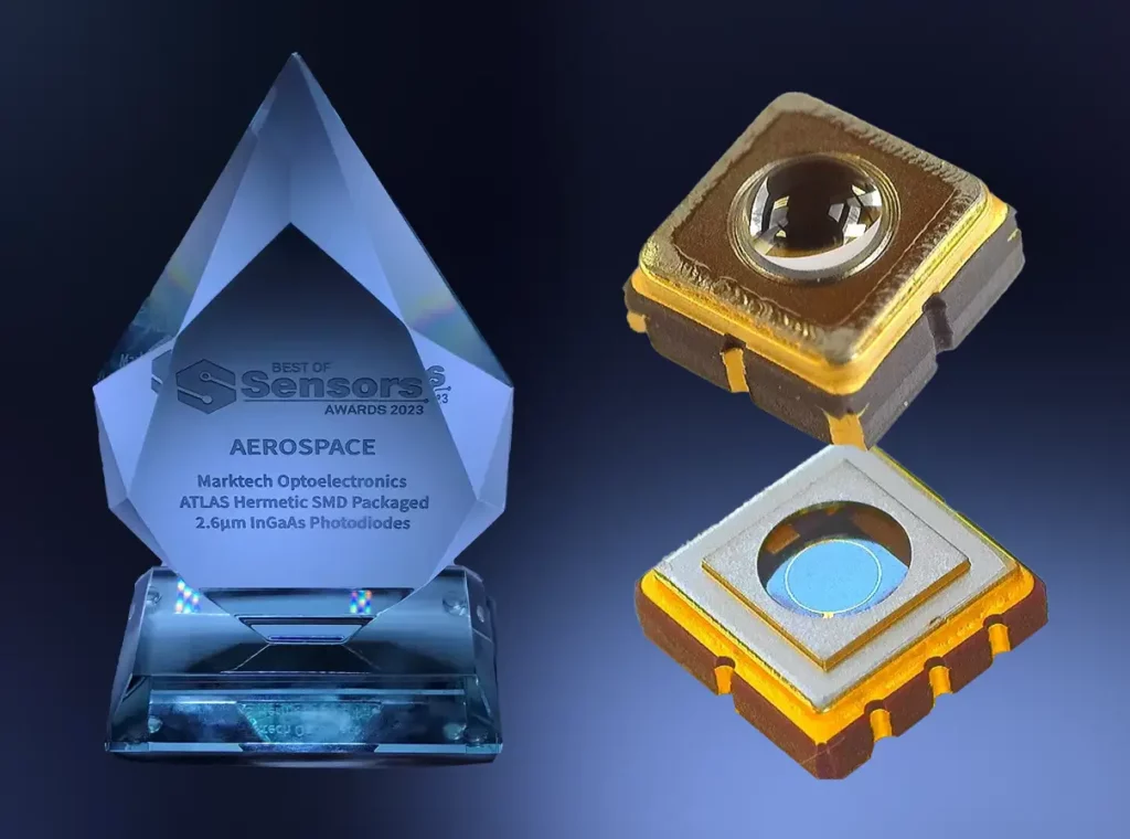
Marktech’s proprietary and award winning ATLAS hermetic metal-ceramic SMD package combines the robustness of hermetic sealing with the convenience of surface mount technology. It’s constructed from metal-ceramic materials to ensure excellent thermal management and hermeticity, making it suitable for high-reliability applications in harsh environments. This type of packaging is often used in military and aerospace industries where device failure is not an option.
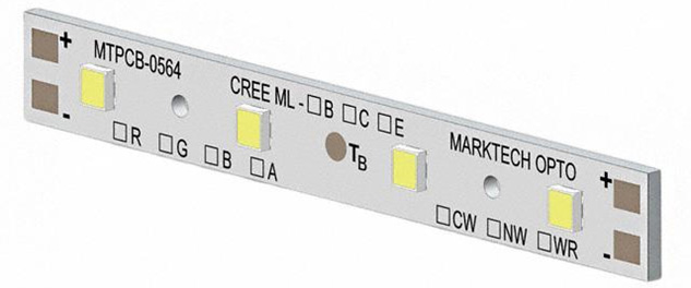
Chip-on-board packaging involves directly mounting the bare semiconductor chip onto the PCB and covering it with protective epoxy or plastic. This approach allows for more efficient use of space and improved heat dissipation. COB packaging is commonly used in LED lighting applications, where multiple LED chips can be placed close together on the same board to create a single, high-intensity light source. Marktech’s COB assemblies can be made with standard FR-4 materials, metal core (aluminum or copper) PCBs, ceramic, and flexible Polyimide. After the die is attached to the board and wire bonded or solder, then a protective encapsulant is applied to provide electrical insulation and protection against moisture and corrosion.

Marktech Optoelectronics exhibits a remarkable capability in multi-chip packaging, offering a versatile range of configurations to meet diverse application needs. This includes packaging multiple LED chips, each emitting different wavelengths, within a single unit, thereby catering to applications requiring a spectrum of light outputs. Furthermore, Marktech can integrate multiple photodiode chips—spanning materials like silicon, InGaAs, and SiC—into a singular package for advanced sensing solutions. Perhaps most notably, they offer the innovative option to combine multiple wavelength-emitting dies with one or more photodiode detectors in the same package. This unique combination facilitates simultaneous emission and detection of light, opening new avenues for compact and efficient optoelectronic devices.

Marktech Optoelectronics stands out in the field of LED technology with its advanced manufacturing capabilities for a wide array of LED assemblies. This includes the production of Star Boards, Linear Boards, and Light Rings, among many other configurations, tailored to meet the specific needs of diverse applications. Their expertise extends to designing and fabricating LED solutions that are both versatile and innovative, ensuring high performance and reliability. Whether for specialized analytical instruments, lighting projects, industrial applications, medical diagnostics, wearables, or consumer electronics, Marktech’s ability to produce various LED assemblies speaks to its commitment to quality and customization. By leveraging state-of-the-art technology and a deep understanding of optoelectronic components, Marktech is adept at delivering solutions that push the boundaries of what’s possible with LED illumination and signaling devices.

Marktech specializes in airtight packaging or optoelectronic components, and for good reason. Packaging integrity is paramount in electronic manufacturing, especially when components are exposed to harsh or demanding environments. Hermetic packaging, particularly glass-to-metal sealed TO cans, stands out as a superior solution, offering unmatched protection for sensitive electronics against the detrimental effects of hydrogen and water vapor infiltration. These intrusions can severely compromise the performance and reliability of encapsulated components, leading to issues such as chemical corrosion, electrical leakage, and even changes in transmission line impedance. These problems not only affect the immediate functionality of the device but can also significantly shorten its lifespan.
Hydrogen and water vapor inside a package can have disastrous consequences for sensitive electronics. For instance, moisture can induce chemical corrosion, damaging metal interconnects crucial for the device’s electrical integrity. Additionally, electrical leakage across the pins or shorts caused by the dendritic growth of metals like silver and gold can disrupt the device’s operation, leading to failure. In photonics, the precision of light transmission is critical; however, this can be compromised by light scattering or wavelength drift caused by internal contaminants.
To counteract these risks, glass-to-metal sealing technology is optimal for manufacturing vacuum-sealed hermetic packages. This method has been trusted for decades thanks to its ability to offer reliable hermeticity — a seal that effectively blocks the entry of gases and moisture. Unlike non- or quasi-hermetic polymer packaging, which might succumb to outgassing or permeation over time, glass-to-metal sealed packages are impervious to such degradation.
The significance of choosing the proper packaging method cannot be overstated for applications that require the utmost reliability and longevity of electronic components. Glass-to-metal sealed TO can provide a robust barrier against environmental threats, preserving sensitive electronics’ integrity, performance, and reliability. This makes them the ideal choice for industries where failure is not an option, from aerospace and defense to medical devices. In the face of challenging conditions, hermetic packaging is not just a protective measure; it’s a crucial investment in the durability and dependability of high-precision electronic devices.
Marktech Optoelectronics specializes in high-integrity hermetic packaging of photodiode detectors, LED emitters, and other optoelectronic devices. The goal is to protect sensitive optical components from environmental conditions while ensuring light can enter or exit the package. Hermeticity or gas tightness is essential in many aerospace, medical, industrial, and mission-critical applications. Detector or emitter chips degrade when exposed to oxygen, moisture, water vapor, and other gases. A hermetic package maintains the reliability and performance of photonic devices over time. Non-hermetic packages can outgas over time when organic compounds volatilize in low vacuum environments such as in vacuum chambers or outer space. Vacuum-tight hermetic packages can be filled with inert gases such as nitrogen or argon to improve vacuum and low-pressure protection.
The hermetic optoelectronic or photonic packaging process consists of several steps:
The die attach process is the first step, where the semiconductor die (or chip) is mounted onto the substrate or lead frame within the TO-can package. This step is crucial for both mechanical support and electrical connection. A conductive or non-conductive adhesive is used depending on the application’s thermal and electrical requirements. For devices that require efficient heat dissipation, such as high-power lasers or LEDs, a silver-filled epoxy or eutectic solder is commonly used to form a bond that aids thermal management.
Following the die attach, wire bonding connects the semiconductor die to the package’s leads (pads or pins), ensuring electrical connectivity. This is typically done using thin gold or aluminum wires. This step uses two primary techniques: ball bonding and wedge bonding. Ball bonding uses a fine wire, usually gold, formed into a ball at one end using a flame or electric arc, which is then bonded to the die and the lead frame. Wedge bonding, on the other hand, can use either gold or aluminum wire pressed down at both the die and the lead connection points using a wedge-shaped tool. This step is critical for the device’s performance, ensuring the electrical signals can be transmitted to and from the semiconductor die.
The final step in the TO-can packaging process is sealing the cap or lens over the package’s open end, creating an airtight seal that protects the internal components from moisture, dust, and other contaminants. This can be achieved through various methods, including welding, soldering, or using glass-to-metal seals. For optoelectronic devices where light transmission is essential, a transparent lens may be used as the cap, allowing for the emission or reception of light while still protecting the internal components. This sealing process is critical for ensuring the long-term reliability of the device, particularly in harsh environmental conditions.
Each step in the hermetic TO-can packaging process is meticulously performed to ensure the optoelectronic device’s functionality and durability. Die to attach, wire bonding, and cap or lens sealing are fundamental to the device’s performance and longevity.
The lens caps used in the packaging process have the optical window or lens bonded to the metal cap using a low-melting-point sealing glass. This glass is also used to form a hermetic, electrically insulating seal around the lead pins in the stem.

What chip mounting options are best suited for your application? More straightforward wire-bond techniques and conductive paste die attach are acceptable for low-power devices. Still, increased thermal conductivity is needed to help lower chip temperatures as power increases.
(Source: Hybond, a wire bonder manufacturer):
There are three types of wire bonding:
A process involving force, time, and heat to join the two materials by inter-diffusion. The wire (heated in some cases) is pressed against the hot surface (at 150° C or more) at high force for a limited period to achieve the bond. No friction is used. This process uses gold wire and a gold bond surface, and it was initially associated with ball bonding. Some still use “thermocompression bonding” as a synonym for ball bonding, even if it now uses ultrasonic friction.
A process involving force, time, ultrasonics, and heat to join two materials. The wire (heated in some cases) is pressed against the hot surface (at 150° C or less) at low force and vibrates for a limited period to achieve the bond. This process uses gold wire and a gold bond surface, and it was also associated initially with ball bonding because the first time ultrasonics were used as a bonding parameter, it was done with ball bonding.
It is so named because it is the bonding of a gold wire, which, in its initial stage, has a ball or sphere formed on the end. A “flame-off” is used to make the ball. Initially, the flame-off was done with an open hydrogen flame, which would rotate towards the end of the wire and melt it, creating a sphere at the end of the wire. Currently, the ball is made with an EFO (electronic flame-off), which creates a spark to melt the end of the wire. This bonding process uses force, time, ultrasonics, and heat to make bonds. In recent years, copper wire has begun to be used for this process, but equipment must be modified to prevent oxidation of the wire, especially the ball, during its formation at flame-off.
Wedge bonding: This process was originally exclusive to aluminum wire, and no heat was used to create bonds. With time, heat was added to the bonding surface, and gold wire was used for thermionic wedge bonding of the gold wire. This is now a common form of bonding gold wire or ribbon. It should be noted, however, that some people still use the phrase “wedge bonding” as a term for ultrasonic (explained below) and not thermosonic wire bonding. Regardless of the traditional meaning of “wedge bonding,” the thermosonic wedge bonding process uses force, time, ultrasonics, and heat to make bonds.
A process that involves the use of force, time, and ultrasonics to join two materials. The wire is pressed against the surface (both at ambient temperature) at low force and vibrated for a limited period to achieve the bond. This process can be done with gold, aluminum, copper, palladium, silver, or platinum wire or ribbons and to bond surfaces of the same materials. Initially, this form of wire bonding was done only with aluminum wire, so to this day, there are still some people who will use the phrase “ultrasonic bonding” as a synonym only for aluminum wire wedge bonding, even if it now is used for gold wire wedge bonding and other materials as well.
This process uses force, time, and ultrasonics with the bonding surface at room/ambient temperature to make bonds. Although originally exclusive to aluminum bonding applications, today, many other materials and alloys can be bonded by the ultrasonic method, including some thought at one time only to be effective if the heat was applied.
This process uses force, time, and ultrasonics with the bonding surface at room/ambient temperature to make bonds. Although peg bonding is the same as wedge bonding and can be done thermosonically and ultrasonically, the main difference with the techniques described earlier is that in a peg bonder, wire is not fed from a spool of wire by the wire bonder. Instead, the wire or ribbon (or any conductor in general) is either pre-aligned over the bond pad or manually introduced under the bonding tool (peg) to be bonded. TAB (tape automated bonding) or single-point TAB is a more common name for this process. Hybond has given the name “peg” to this type of bonding because naming it TAB would lead to the assumption that a tape-feeding mechanism would be included as part of the equipment, and in reality, it is not. Hybond also gives the name peg because the tool used for bonding usually looks like a peg, just as the tool used in wedge bonding looks like a wedge.
Today, ultrasonic bonding is a different process from what it was initially thought to be. The concept of interfacial rubbing is not valid. Ultrasonic energy, when applied to the metal to be bonded, renders it temporarily soft and plastic. This causes the metal to flow under pressure. The acoustic energy frees molecules and dislocates them from their pinned positions, which allows the metal to flow under the low-compressive forces of the bond. Thus, heat at the bond site becomes a byproduct of the bonding process, and the external heat becomes unnecessary to form the bond. This is also called a “cold weld.”
The wire’s friction breaks up and sweeps aside some contaminants in the weld area, exposing clean metallic surfaces that promote metallurgical bonds. It is essential, however, to begin with a clean surface to avoid difficulties or failures in bonding. In some cases, the ultrasonic scrubbing may not be able to remove contaminants, as in the case of lubricants.
It also was found that the bonding tool moves cyclically across the top of the wire. A regular flat tool may not grip the wire well enough, and this causes the wire to slip back and forth across the bond surface of the tool. For this reason, tools are made with more porous materials, such as ceramic-metal alloys, or special features like cross grooves or grids that assist in gripping the wire during ultrasonic and thermosonic bonding.
The viewing angle of an LED, which determines how wide the light is dispersed from the LED, varies significantly based on the type of lens or package the LED is housed in. Here’s a general overview of the typical viewing angle ranges for LEDs packaged in flat lens, dome lens, and ball lens configurations:
Flat lens LEDs are designed to spread light over a wide area, making them suitable for applications with a broad illumination pattern. The typical viewing angle for flat lens LEDs can range from 120° to 160°. These broad angles are achieved because the flat surface does not focus the light, allowing it to disperse more broadly.
Dome lens LEDs feature a rounded lens that helps focus the light, resulting in a narrower beam of light than flat lens LEDs. The typical viewing angle for dome lens LEDs ranges from 20° to 60°. This configuration is often used when a more focused light beam is required, such as in flashlight applications or for spotlighting.
Ball lens LEDs have a spherical lens, offering a unique combination of focus and dispersion. The typical viewing angle for ball lens LEDs can vary widely based on the exact design of the lens and the LED’s intended application. Generally, the viewing angles for ball lens LEDs can range anywhere from 5° to 45°, with some designs possibly extending slightly beyond this range. Ball lens LEDs are often used in applications where precision optical performance is needed.
It’s important to note that several factors, including the design of the LED package, the material of the lens, and the intended use-case, can influence the viewing angle. Manufacturers often provide detailed specifications for each LED model, including the exact viewing angle, to help designers choose the right LED for their application.
Let us help select the perfect parts and services to make your application come to life.

Do you need a small number of LEDs for your proof of concept? Or, are you looking to purchase a run for your prototypes? Visit our online stores at Digi-Key Electronics and Mouser Electronics today. In Japan, our products are now available through Rikei Corporation. In Israel, our products are now available through Militram. In Canada, our products are now available through ARL Group.

As our industry constantly changes and evolves, Marktech has been there since the start. Stay on top of new and upcoming technology trends, industry news and new product offerings.
Marktech Optoelectronics
3 Northway Lane North
Latham, NY 12110
Fax: +1-785-4725
Email: in**@ma**********.com